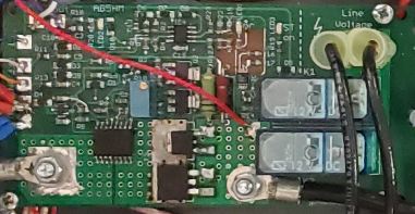
DC Safet Switch
The purpose of the DC safety switch is to disconnect and protect the LDMOS devices from the high power
DC source in case something goes wrong. This is important since the the DC power supplies are strong
enough to weld... i don't want to exaggerate, but this could cause even more damage or start a fire.
After some research i found out that most of the designs out there are based on an automotive high-side
switch (BTS50085) from Infineon. Unfortunately, this device can only be used up to 55Vdc.
I was unable to find a design, suitable for 65V with the necessary safety features.
So i had to come up with my own design.
During my development, i had quite some instances where the switch triggered, but i never lost an
LDMOS device so far.
This switch incorporates the following functionalities:
Functional Description
For over current protection and current sense i used the integrated current sensor MLX91220 from Melexis.
It incorporates and Hall current sensor and adjustable overcurrent logic.
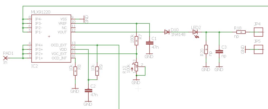
PAD1 is the positive input from the power supply and the current is fed through the IC and exits on pin 5..8.
The overcurrent shutdown limit can be adjusted with R10 from 35...50A.
Pin 13 provides the over current shutdown signal and turns low when the current is above the setpoint.
Pin 12 provides an analog readout of the current. Since the IC is able to measure bipolar currents, the output
of this signal has an 2.5V offset. D10 and LED2 are used to reduce this offset to about 0.35V on JP4.
Linearization of this signal is then done in the controller software.
I decided to use N-channel MOSFETs due to their lower Rds(on) instead of P-channel FETs for lower losses in
the FETs and therefore no need of an heatsink. The drawback is that the Gate voltage of an N-channel FET needs
to be higher than the Drain - Source voltage (63V in my case).
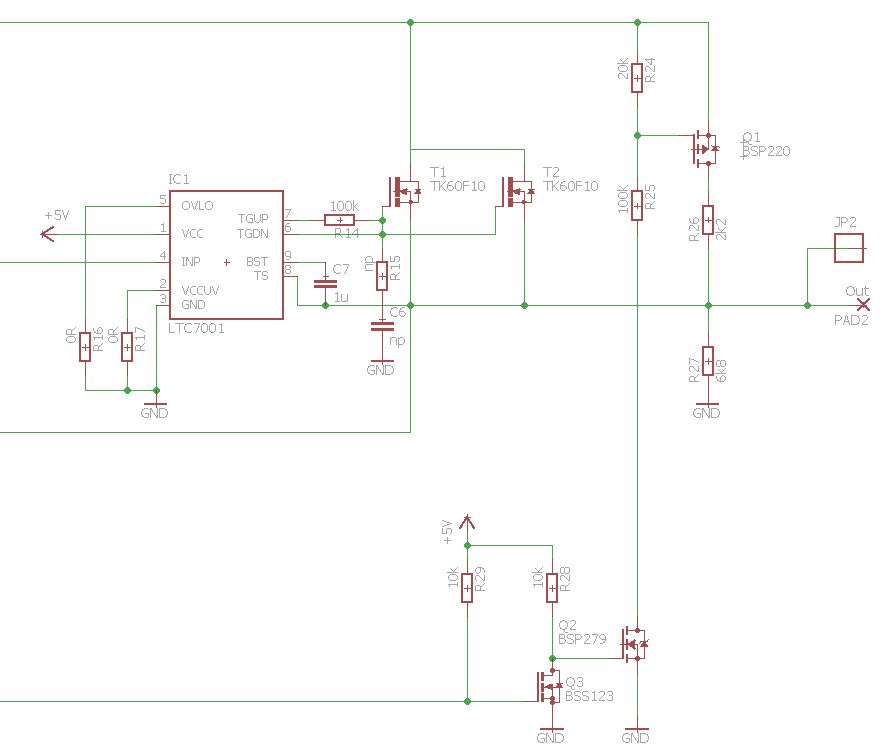
IC1 is a charge pump that provides a Gate that is around 14V above the Drain-Source voltage that is then fed to
the main FETs T1 and T2 when a 5V high signal is applied to pin 4 of IC1.
Q1 and R26 are the soft start circuit to limit the inrush current due to the capacitors in the PA module.
Q2 and Q3 are used to shift the Gate voltage down from 65V to 5V without reversing the logic. A low signal on the Gate
of Q3 will turn Q1 on and start to charge up the capacitors in the PA module.
The control logic is made of two operational amplifier.
IC4A is a Schmitt-Trigger to ensure staple switching states, while IC4B is an inverted amplifier to monitor
the output voltage.
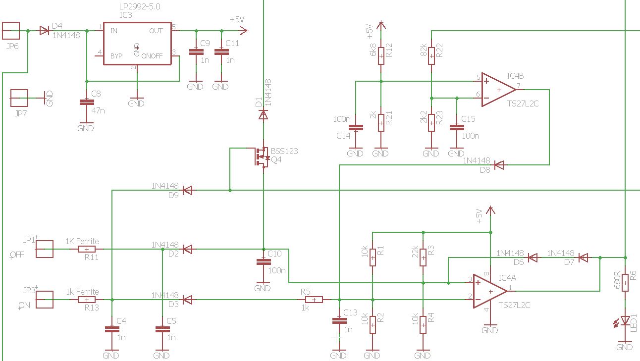
R4 and C10 have a higher value than R1..R3 and C13 to ensure that the switch stays in OFF mode during
voltage buildup on the input.
When JP3 (on) is pulled to ground, the pre charge circuit is activated through D4. Once the voltage reaches
around 35V, the output of IC4B turns low and enables IC4A to switch into high state and the T1 and T2 will
be switched on.
In case of an short circuit on the output side, the voltage won't build up to 35V and switch won't turn on.
While JP3 (on) is pulled to ground, Q4 turns off and disable the over current shutdown of IC2.
This prevents false triggering of the switchover from pre charge to ON mode.
Once the ON state is active, JP3 needs to be set to high state to enable the over current protection.
When JP1(off) is pulled to ground, IC4A goes to low state and T1 and T2 are switched off.
This PCB incorporates also relays the soft start resistor of the main power supply to reduce inrush current.
I decided to use two relays in parallel since standard PCB relays usually are only rated up to 16A which
will be to less if you decide to operate the amplifier at 120Vac.
Once the PA controller has booted, it will turn these relays on to short the soft start resistor.